Samsung is set to begin making chips utilizing its 2 nd Generation 3nm-class (SF3) production innovation along with performance-enhanced variation of its 4nm-class (SF4X) fabrication procedure in the 2nd half of next year, the business informed its financiers today. Both production nodes are anticipated to substantially enhance competitive positions of the business as they will allow it to construct brand-new kinds of items.
” We will reinforce our innovation competitiveness through the 2H [2024] mass production of the second generation 3nm procedure along with the 4 th generation 4nm procedure for HPC,” a declaration by the business checks out. “The marketplace is anticipated to move to development thanks to a rebound in mobile need and continued development in HPC need.”
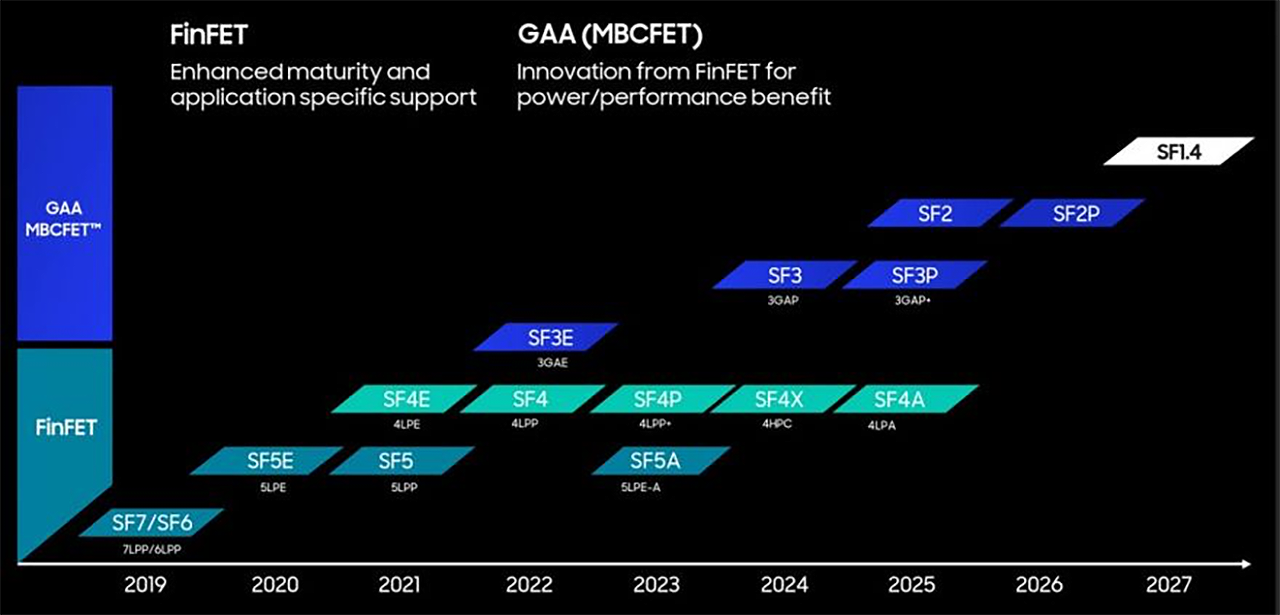
Samsung’s upcoming SF3 procedure innovation is a significant upgrade to its existing SF3E production node, which, based upon the offered understanding, is just utilized to make little chips for cryptocurrency mining. Samsung asserts that the SF3 will use higher style flexibility by permitting various gate-all-around (GAA) transistor’s nanosheet channel widths within the exact same cell type.
Although Samsung does not make direct contrasts in between SF3 and SF3E, it states that SF3 provides significant enhancements over SF4 (4LPP, 4nm-class, low power plus), that includes a 22% boost in efficiency at comparable power and intricacy, or additionally, a 34% decrease in power usage at the exact same frequency and transistor count, in addition to a 21% decrease in reasoning location. In basic, it is anticipated that SF3 will be a much better choice for intricate styles than SF3E, though it will get in high-volume production in the 2nd half of 2024.
In the meantime, Samsung Foundry’s 4nm-class generation nodes continue to progress. The business getting ready to release its SF4X (4HPC, 4 nm-class high-performance computing) procedure innovation, customized for high-performance applications such as CPUs and GPUs utilized in information centers. This one is going to be SF’s very first procedure node in current years that has actually been particularly created for high-performance computing (HPC) applications.
Samsung’s SF4X procedure innovation guarantees to provide a 10% enhancement in efficiency in addition to a 23% decrease in power usage. While Samsung has not divulged the standard for this contrast, it is most likely in referral to their basic SF4 (4LPP) procedure. This improvement is attained through a redesign of the transistor’s source and drain areas, following a reassessment of their efficiency under possibly high-stress conditions, the application of innovative transistor-level design-technology co-optimization (T-DTCO), and the execution of a brand-new middle-of-line (MOL) architecture.
With improved MOL architecture, SF4X is anticipated to accomplish a silicon-validated minimum operating voltage (Vmin) for CPUs at 60mV, lower the irregularity in the off-state present (IDDQ) by 10%, make sure steady high voltage (Vdd) operation above 1V without jeopardizing efficiency, and improve procedure margin for SRAM.