Samsung’s yearly Memory Tech Day is occurring in San Jose today, and as part of the occasion, the business is making a number of noteworthy memory innovation announcements/disclosures. The emphasize of Samsung’s occasion is the intro of Shinebolt, Samsung’s HBM3E memory that will set brand-new marks for both memory bandwidth and memory capability for high-end processors. The business is likewise divulging a bit more on their GDDR7 memory, which will mark a substantial technological upgrade to the GDDR household of memory requirements.
Beginning things off, we have today’s marquee statement: Shinebolt HBM3E memory. Like the remainder of the memory market, Samsung is preparing a follower to the current-generation of HBM3 memory that’s being utilized with high-end/HPC-grade processors, with the market settling around the upcoming HBM3E requirement HBM3E is slated to use both considerably greater capabilities and higher memory bandwidth than HBM3, assisting the high-bandwidth memory innovation stay up to date with ever-growing work on high-end processors.
| Samsung HBM Memory Generations | ||||||
| HBM3E ( Shinebolt) |
HBM3 ( Icebolt) |
HBM2E ( Flashbolt) |
HBM2 ( Aquabolt) |
|||
| Max Capability | 36GB | 24 GB | 16 GB | 8 GB | ||
| Max Bandwidth Per Pin | 9.8 Gb/s | 6.4 Gb/s | 3.6 Gb/s | 2.0 Gb/s | ||
| Variety Of DRAM ICs per Stack | 12 | 12 | 8 | 8 | ||
| Efficient Bus Width | 1024-bit | |||||
| Voltage | ? | 1.1 V | 1.2 V | 1.2 V | ||
| Bandwidth per Stack | 1.225 TB/s | 819.2 GB/s | 460.8 GB/s | 256 GB/s | ||
The basis of Shinebolt is a brand-new 24Gbit HBM memory pass away, which Samsung will be producing on their D1a procedure, the business’s EUV-based 4 th generation 10nm-class (14nm) node. Samsung will be producing both 8Hi and ultimately 12Hi stacks based upon this brand-new die, permitting overall stack capabilities of 24GB and 36GB respectively, 50% more capability than their HBM3 (Icebolt) equivalents.
According to Samsung, Shinebolt will have the ability to strike memory clockspeeds as high as 9.8 Gbps/pin, much better than 50% faster than their HBM3 items. Though provided a few of Samsung’s previous memory clockspeed claims, there’s a likelihood this is a semi-overclocked state. Shinebolt advancement isn’t far enough along for Samsung to note private SKUs, however even at the conservative end of things, Samsung is promoting information rates of a minimum of 8Gbps/pin in their occasion news release. And if Samsung’s enthusiastic memory frequencies do concern fulfillment, then that would put Samsung ahead of their competitors too; to date, SK hynix and Micron have actually revealed prepare for 9Gbps/pin and 9.2 Gbps/pin memory respectively, so Samsung’s claims are definitely the most aggressive.
In general, these clockspeeds would provide a single HBM3E stack a minimum bandwidth of 1TB/sec, and an optimum bandwidth of 1.225 TB/sec, well ahead of the 819GB/sec information rate of HBM3. Or to frame things in recommendation of a high-end processor (e.g. NVIDIA H100), a 6-stack chip would have the ability to gain access to as much as 216GB of memory with an aggregate memory bandwidth as high as 7.35 TB/sec.
When it comes to power effectiveness, things seem a little a variety. On a relative basis, Samsung states that Shinebolt will be 10% more effective than Icebolt– simply put, taking in 10% less power per bit moved (pJ/bit). Nevertheless, a 25%+ clockspeed enhancement will more than erase those gains due to the substantial boost in bits moved. So while Shinebolt will be more effective total, on an outright basis it appears that overall power usage for HBM memory will continue to grow with the next generation.
In either case, for the high-end processor market that Samsung is targeting with Shinebolt, chipmakers are not likely to be fazed by the power boost. Like the remainder of the high-end processor area, Samsung has the AI market set square in its sights– a market sector where both memory bandwidth and memory capability are restricting aspects, particularly with huge big language designs (LLMs). In addition to the conventional supercomputer and networking market sectors, Samsung ought to have little problem offering quicker HBM in the middle of a flourishing AI market.
Like the other significant memory suppliers, Samsung anticipates to deliver Shinebolt at some time in 2024. Considered that the business simply began tasting the memory– which HBM3 Icebolt itself simply struck mass production– Shinebolt’s most likely not delivering up until the later part of the year.
A Short Teaser on HBM4: FinFETs & & Copper-to-Copper Bonding
Lastly, looking even further into the future, Samsung is quickly speaking about their prepare for HBM4 memory. While that innovation is still a couple of years off (there’s not even an authorized spec for it yet), we understand from previous disclosures that the memory market is intending to transfer to a larger, 2048-bit memory user interface. Which, as Samsung likes to frame things, is the only useful option when even more HBM clockspeed boosts would burn out power usage.
For HBM4, Samsung is taking a look at utilizing advanced fab and product packaging innovations that are presently the domain of reasoning chips. On the fabulous side of matters, the business wishes to transfer to utilizing FinFET transistors for their memory, rather than the planar transistors still utilized there. Just like reasoning, FinFETs would minimize the drive present needed, which would assist to enhance DRAM energy effectiveness. On the other hand on the product packaging side of matters, Samsung is taking a look at moving from micro-bump bonding to bumpless (direct copper-to-copper) bonding, a packaging strategy that’s still on the cutting-edge of advancement even in the reasoning area. Welcoming advanced innovations will be vital to keeping HBM bandwidth growing as it has more than the last years, however the expenses and intricacies of doing so likewise highlight why HBM stays a specifically specific niche high-end memory innovation.
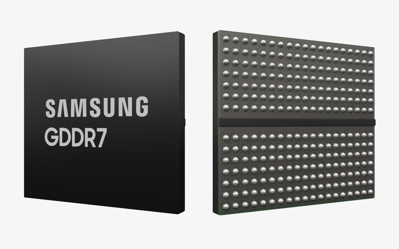
GDDR7 Update: 50% Lower Stand-By Power Than GDDR6
Besides HBM3E, Samsung’s other huge bandwidth memory upgrade of the day is a quick status upgrade on their GDDR7 memory.
Back in July of this year, Samsung revealed that they finished preliminary advancement on their GDDR7 memory The next generation of GDDR memory, GDDR7 brings with it numerous significant modifications versus today’s GDDR6, the most substantial of which is a switch to PAM3 encoding. PAM3 enables 1.5 bits to be moved per cycle (or rather 3 bits over 2 cycles), unlocking to enhancing memory transfer rates without utilizing more pricey methods of additional enhancing the frequency of the memory bus.
| GDDR Memory Generations | |||||
| GDDR7 | GDDR6X | GDDR6 | |||
| B/W Per Pin | 32 Gbps (Forecasted) | 24 Gbps (Shipping) | 24 Gbps (Testing) | ||
| Chip Density | 2 GB (16 Gb) | 2 GB (16 Gb) | 2 GB (16 Gb) | ||
| Overall B/W (256-bit bus) | 1024 GB/sec | 768 GB/ssec | 768 GB/ssec | ||
| DRAM Voltage | 1.2 V | 1.35 V | 1.35 V | ||
| Data Rate | QDR | QDR | QDR | ||
| Signaling | PAM-3 | PAM-4 | NRZ (Binary) | ||
| Product Packaging | 266 FBGA | 180 FBGA | 180 FBGA | ||
As a fast wrap-up from Samsung’s July statement, Samsung will be presenting 16Gbit (2GB) modules, which will have the ability to perform at as much as 32Gbps/pin. That’s a 33% enhancement in bandwidth per pin over present GDDR6 memory, and would bring the aggregate bandwidth of a 256-bit memory bus to a cool 1TB/second. GDDR7 ought to likewise provide a 20% enhancement in power effectiveness over Samsung’s GDDR6 (in regards to pJ/bit), thanks in part to using Samsung’s 3 rd generation D1z (10nm-class) fab node.
Today’s occasion from Samsung is mostly a wrap-up of July’s statement, however at the same time we have actually found out a number of brand-new technical information on GDDR7 that Samsung hasn’t formerly divulged. To begin with, GDDR7 isn’t simply enhancing active power usage, however the tech will likewise enhance on stand-by power usage to a substantial degree. Thanks to extra clock controls, GDDR7 will take in 50% less stand-by power than GDDR6.
2nd, in going over why Samsung (and the market as a whole) chose PAM3 encoding for GDDR7 rather of even denser PAM4, the business validated a few of our technical suppositions on the brand-new innovation. In other words, PAM3 has a lower typical bit mistake rate (BER) than PAM4, mostly thanks to the broader margins on the eye window. None of that makes PAM4 unfeasible (as Micron has actually currently shown), however Samsung and the rest of the memory market are preferring the relative simpleness of PAM3, provided the compromises.
Besides the normal video card/gaming clients, Samsung is anticipating GDDR7 to be embraced by AI chip makers, and possibly a bit more remarkably, the vehicle market. In truth a few of these non-traditional clients might be the very first to embrace the memory; given that the conventional GPU suppliers are still mid-cycle on their present generation of items, it will still be rather a long time before they deliver any GDDR7-capable silicon.
At this moment Samsung has actually not revealed a forecasted date for when their GDDR7 memory will enter into mass production. However the business is still anticipating that they will be the very first supplier to deliver the next-generation memory, most likely in 2024.